About
- Home
- About
Message from Director Desk
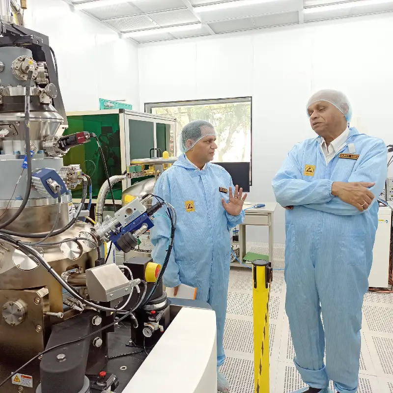
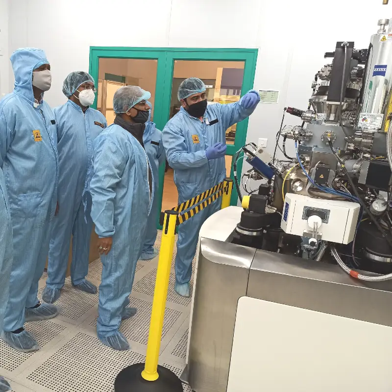
The Centre for Design & Fabrication of Electronic Devices (C4DFED) at the Indian Institute of Technology (IIT) Mandi, Himachal Pradesh, India is a unique world-class facility for multidisciplinary research on electronic device design and fabrication. This center has Class 100, Class 1000 & Class 10000 laboratories where high-end sophisticated electronic device design, fabrication, and characterization tools are installed & housed.
The C4DFED facility is established to acquire both theoretical and practical knowledge of VLSI technology, chip design, testing, and fabrication. Students & research scholars get exposure to VLSI design, testing, and complete device fabrication processes. This equips them to meet the challenging needs of industry for the next generation. This gives our graduates the necessary technical and professional maturity to handle unforeseen challenges in tomorrow’s rapidly changing world. Their appreciation for disciplines other than their own makes them well-suited to work on real-world product and technology development.
I invite you to visit our unique C4DFED @ IIT Mandi facility & this will also be an opportunity to learn about the exciting research being done on our campus and to explore synergies. I look forward to building a long-lasting and mutually beneficial relationship with you.

Message from Coordinator Desk
C4DFED rises from the heart of the Himalayas, a sanctuary where the mountain’s eternal breath meets the delicate pulse of creation, weaving world-class precision into the very fabric of India’s electronic renaissance.
Established in 2018, C4DFED is a premier institute-wide facility dedicated to the design,
fabrication, and characterization of next-generation nano-electronics devices. We house a state-of-the-art Class 100; Class 1000 cleanroom facility equipped with sophisticated lithography, deposition, etching, and characterization tools. By bridging the gap between theoretical physics, material science, and electrical engineering, we provide a platform for researchers and industry partners to translate “lab-scale” concepts into functional prototypes.
C4DFED operates at the frontier of high-impact technology through:
- Innovative Materials: Developing sub-10 nm extreme UV lithography photoresists and 2D layered semiconductors for next-generation electronics.
- Advanced Devices: Engineering high-performance FETs, non-volatile memory, optoelectronics, environmental sensors, flexible organic devices, power devices, and quantum computing junctions
- Strategic Collaborations: Serving as a national mission hub that empowers startups and industry through fabrication, consultancy, and joint R&D.
- Capacity Building: Bridging the semiconductor skill gap via specialized curricula and intensive “hands-on” training workshops.
C4DFED drives high-impact research for the global industry and national progress through
strategic partnerships with government bodies like ISRO, ANRF, DAE-BRNS, and the INAE India-Taiwan program, alongside international industrial leaders such as EMD Merck, USA.
Vision of C4DFED Facility @ IIT Mandi
To be a global leader in semiconductor innovation and sustainable electronics, empowering India’s technological self-reliance through world-class research, cutting-edge fabrication, and visionary talent development.
Mission of C4DFED Facility @ IIT Mandi
Maintenance of a state-of-the-art, centralized facility for the design and fabrication of next-generation integrated circuits, semiconductor devices, & futuristic electronic materials.
Cultivation of highly skilled workforce through specialized interdisciplinary practicum programs to meet the evolving demands of global semiconductor industry.
Foster robust partnerships with industries to enable the translation of laboratory innovations into commercially viable and sustainable technologies.
Serve as a premier national hub that provides training, outreach, and facility access to researchers, educators, and students.
Drive interdisciplinary research and development that aligns with the “Make in India” initiative and addresses the unique challenges of the Himalayan region.