Centre for Design & Fabrication of Electronic Devices
C4DFED at IIT Mandi (Himachal Pradesh), is a unique world-class facility for multidisciplinary research on electronic device design and fabrication.
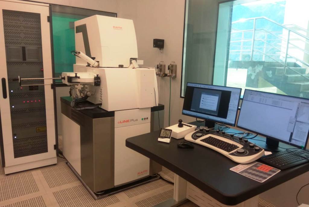
State-of-the-Art Class 100 Clean Room Facility.
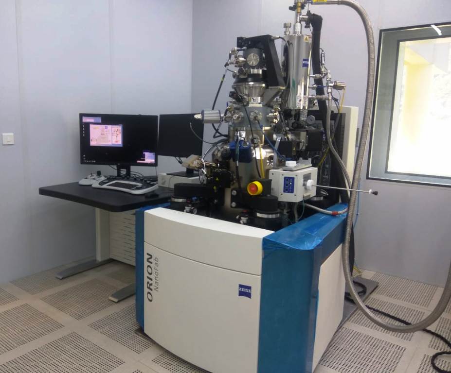
Sub-10 nm Exposure Systems for Lithography.
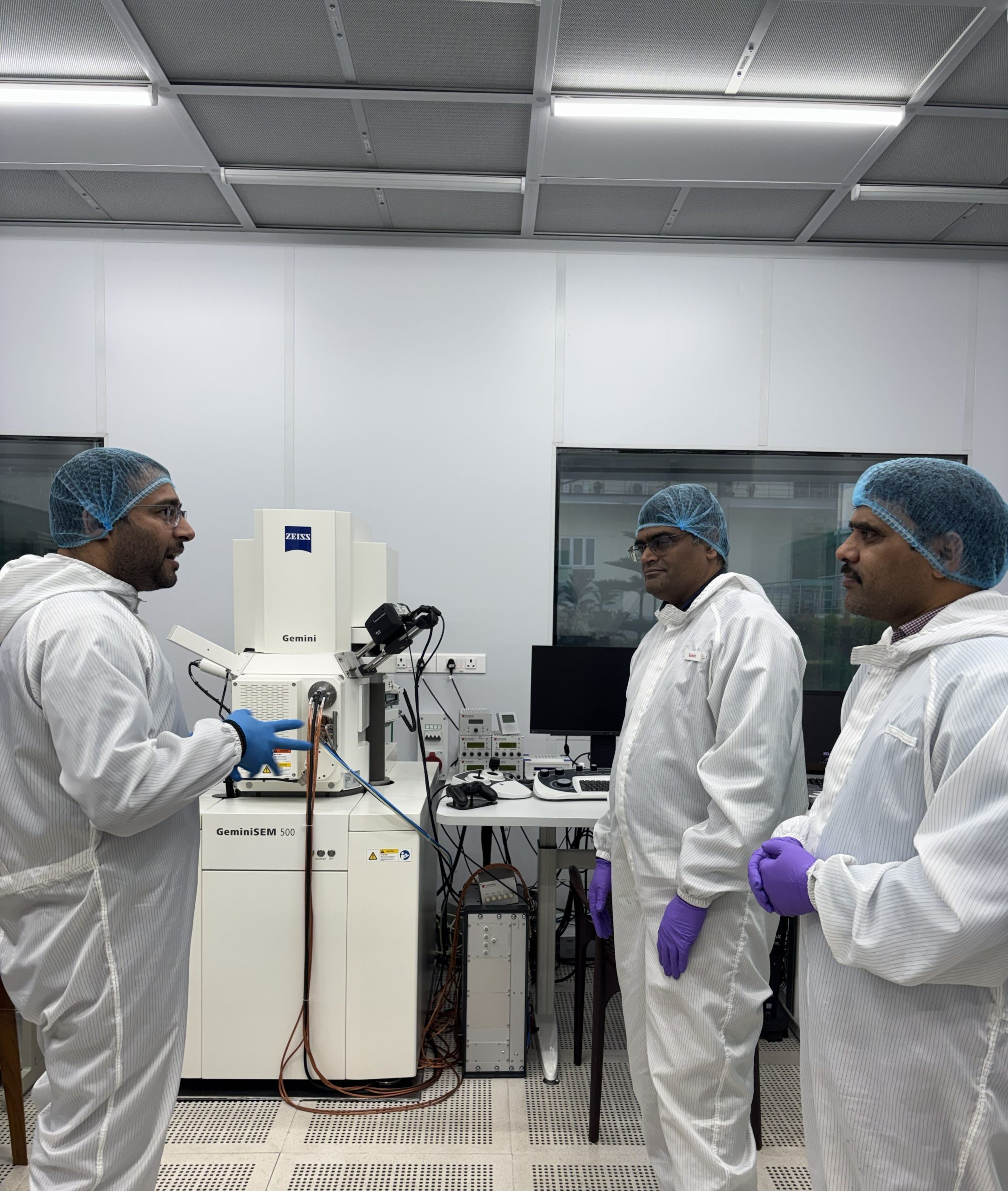
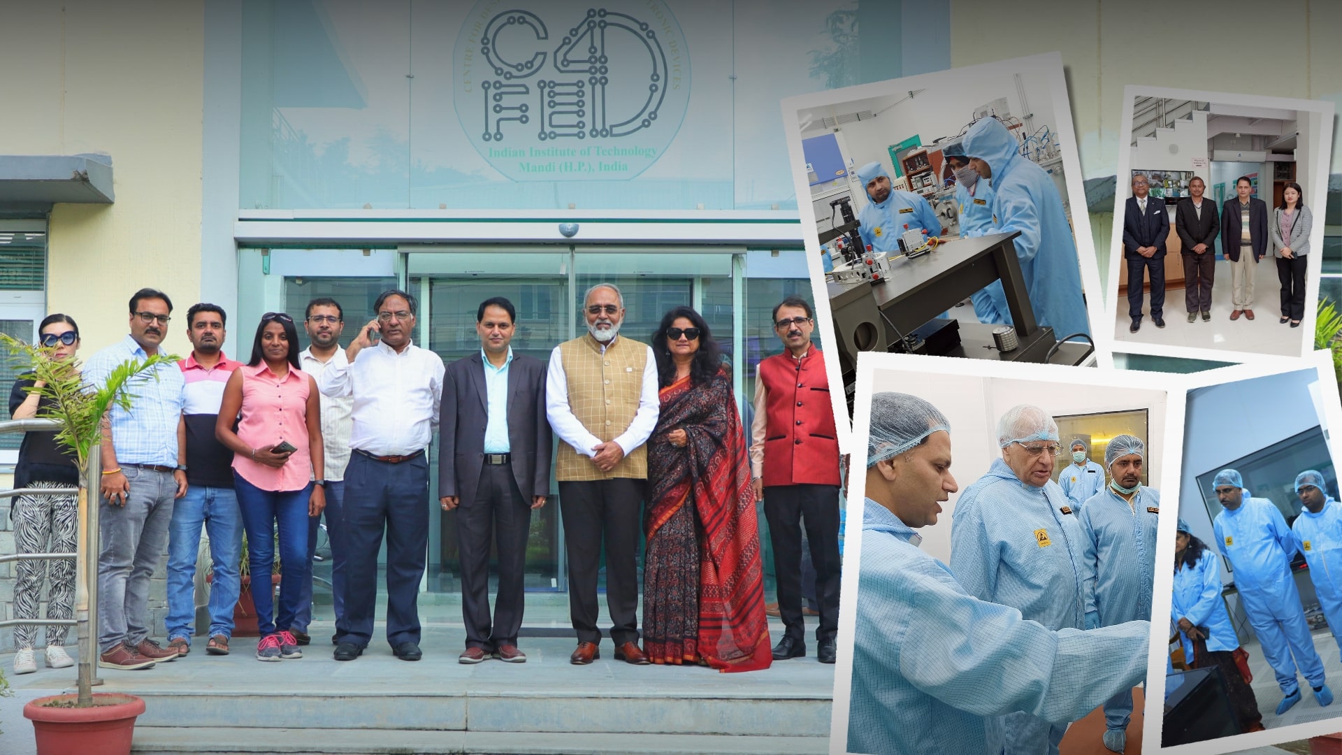
ANRF CEO at C4DFED facility.
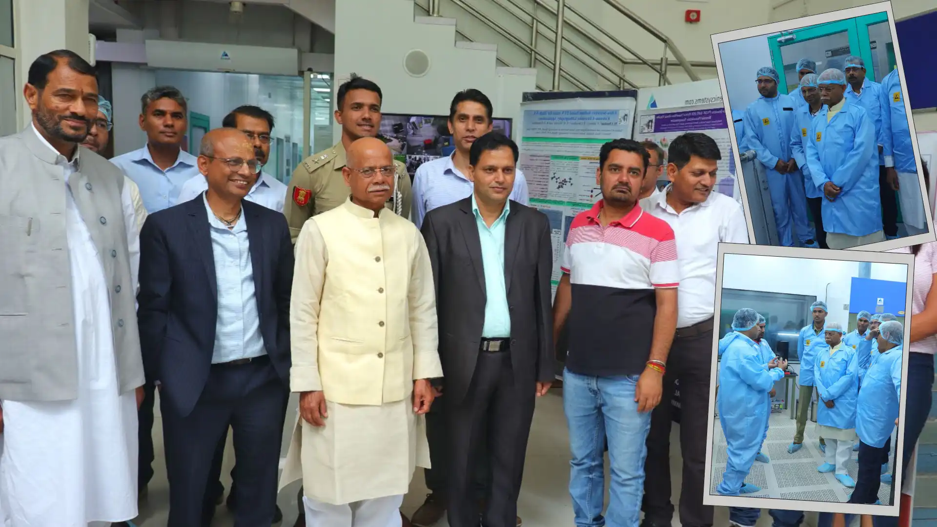
Governor of Himachal Pradesh at C4DFED
Overview
Center for Design & Fabrication of Electronic Devices (C4DFED)
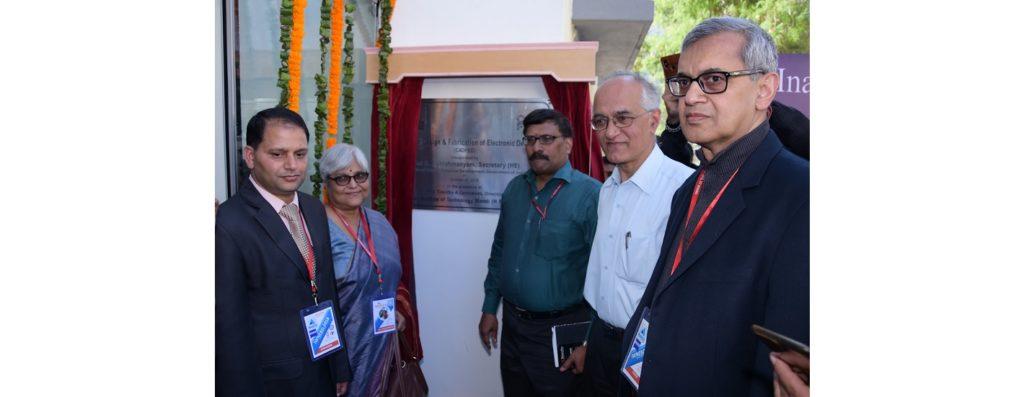
The Centre for Design & Fabrication of Electronic Devices (C4DFED) facility at Indian Institute of Technology (IIT) Mandi is a unique facility for multidisciplinary research on micro-nanoscale semiconductor devices design and fabrication where many state-of-the-art facilities and utilities are housed inside class 100, class 1000 and class 10000 clean laboratories panning nearly 2000 ft2 of area. The high-end state-of-the-art facility was inaugurated by Sh. R. Subrahmanyam, Secretary, Higher Education (HE), Ministry of Human Resource Development (MHRD), and Government of India (GoI) on 31 Oct, 2018.
Events
Announcements
IEEE EDS Summer School on Electronics Device Technology (EDT) June 2026
An intensive five-days summer school to bridge the gap between theory and real-world semiconductor technology, equipping the next-generation of engineers and researchers with hands-on experience on electronics device design, fabrication, and characterization.
C4DFED at IIT Mandi (Himachal Pradesh), is a unique world-class facility for Multidisciplinary Research on Electronic Device Design and Fabrication
Our best pricing plan
Smart And Flexible Pricing Plan For Your Business
The primary goal of business consulting is to help organizations improve their performance, solve specific problems, and achieve their
strategic objectives. Dolor sit amet consectetur.

Satisfied Client ratings
$
89.00
/ Month
- Experienced Peoples
- Competitive Pricing
- Intellect And Experience
- Commitment To Quality
- Experienced Peoples
- Competitive Pricing
- Intellect And Experience
- Commitment To Quality
What is business consulting?
Bring to the table win-win survival strategies to ensure proactive domination. At the end of the day, going forward, a new normal that has evolved from generation Z.

What do business consultants do?
Bring to the table win-win survival strategies to ensure proactive domination. At the end of the day, going forward, a new normal that has evolved from generation Z.

Why do companies hire business consultants?
Bring to the table win-win survival strategies to ensure proactive domination. At the end of the day, going forward, a new normal that has evolved from generation Z.

How much do business consultants charge?
Bring to the table win-win survival strategies to ensure proactive domination. At the end of the day, going forward, a new normal that has evolved from generation Z.

faq
Frequently Ask & Questions For Business
special business consultant
Parturient montes nascetur ridiculus mus is maecenas neque in feugiat elementum lacus risus.
business development
Parturient montes nascetur ridiculus mus is maecenas neque in feugiat elementum lacus risus.
Our Testimonials
Peoples Talk About C4DFED
LOREM TESTIMONIALs

Michael G. Ware
Managing Director
best lorem

Kevin Smith
Customer
lorem

David Anderson
Customer
Latest Blog
Our Latest Blog & News
Call Open for Post-Doc Fellows
C4DFED0 Comments
Call Open for Post-Doc Fellows
C4DFED0 Comments
Sputtering System is Available to use
C4DFED0 Comments
Trusted By Top Companies


