Equipment's list
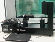
Contact Angle
The purpose is to verify whether the substrate is hydrophobic or hydrophilic in nature.
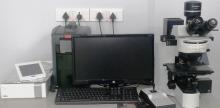
Optical Microscope
This is high end optical microscope with the attached accessories for temperature dependent analysis. This microscope has a resolution of 100x
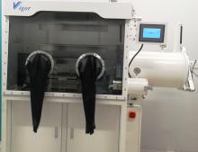
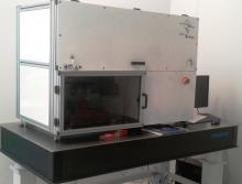
Glove Box
This system is used for the synthesis of the device in the controlled atmosphere of the desired Gas.
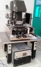
Mask Aligner (Optical Lithography)
Mask Aligner is the mask dependent lithography system depending on the flood exposure of UV light.
Maskless Lithography
This instrument is used for pattering for device fabrication using CAD based Mask. This instrument has the resolution of 5 µm.
Ellipsometry
This instrument can be used for extraction of the dielectric properties as well thickness of the thin film typically of few nm. The instrument relies on the fact that the reflection at a dielectric interface depends on the polarization of the light while
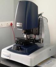
Optical Profilometer
The purpose of profilometry is to get surface morphology, step heights and surface roughness. It is a non-contact technique.

AFM (Atomic Force Microscopy)
Atomic force microscopy (AFM) is a very high-resolution type of scanning probe microscopy, with demonstrated resolution on the order of fractions of a nanometer. The purpose of this instrument is to analyse the surface properties of thin films.
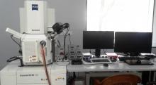
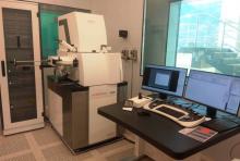
FESEM (Field Emission Scanning Electron Microscope)
Field emission scanning electron microscopy (FESEM) provides topographical and elemental information at magnifications of 10x to 300,000x, with virtually unlimited depth of field. Applications of FESEM include:
Electron Beam Lithography
Electron-beam lithography (often abbreviated as e-beam lithography) is the practice of scanning a focused beam of electrons to draw custom shapes on a surface covered with an electron-sensitive film called a resist. This instrument pattern the substrate