Field emission scanning electron microscopy (FESEM) provides topographical and elemental information at magnifications of 10x to 300,000x, with virtually unlimited depth of field. Applications of FESEM include:
Semiconductor device cross section analyses for gate widths, gate oxides, film thicknesses, and construction details
Advanced coating thickness and structure uniformity determination
The additional attachments with the FESEM allow the electrical characterization of transistor at nanometer level.
Instument image
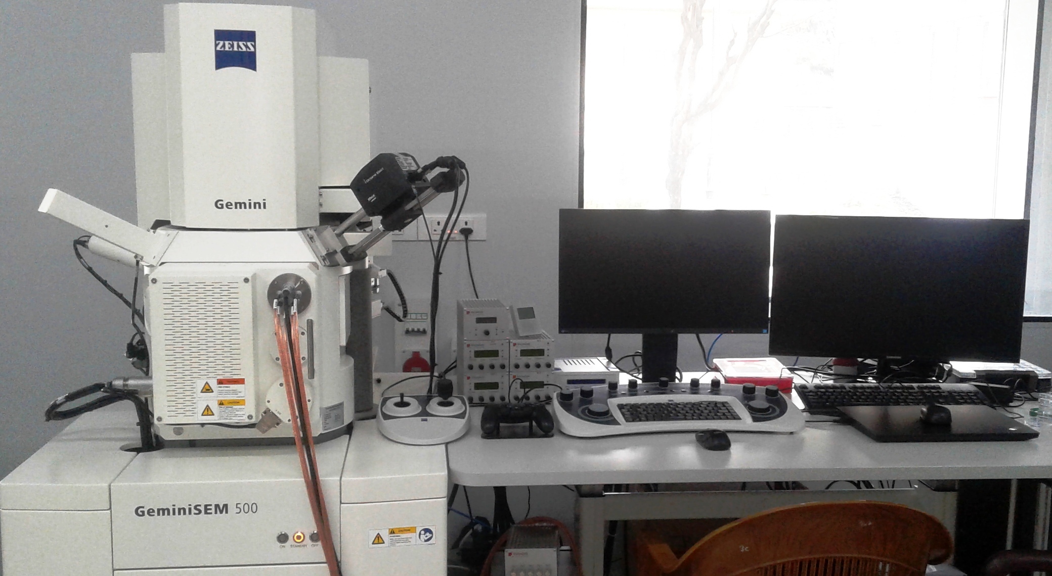
Company
Carl Zeiss Microscope
Model
GeminiSEM 500
Purpose
Field emission scanning electron microscopy (FESEM) provides topographical and elemental information at magnifications of 10x to 300,000x, with virtually unlimited depth of field. Applications of FESEM include: