From the Director's Desk
Greeting from IIT-Mandi, India!

Prof. Laxmidhar Behera
Director, IIT Mandi
The Centre for Design & Fabrication of Electronic Devices (C4DFED) at (IIT) Mandi (Himachal Pradesh), India is a unique world-class facility for multidisciplinary research on electronic device design and fabrication. this center has class 100, Class 1000 & Class 10000 laboratories where high-end sophisticated electronic device design, fabrications, and characterizations tools are installed & housed.
The C4DFED facility is established to acquire both theoretical and practical knowledge of VLSI technology, chip design, testing, and fabrication. Students & research scholars get exposure to VLSI design, testing, and complete device fabrication processes. This equips them to meet the challenging needs of industry for the next generation. This gives our graduates the necessary technical and professional maturity to handle unforeseen challenges in tomorrow's rapidly changing world. Their appreciation for disciplines other than their own makes them well-suited to work on real-world product and technology development.
I invite you to visit our unique C4DFED @ IIT Mandi facility & this will also be an opportunity to learn about the exciting research being done on our campus and to explore synergies. I look forward to building a long-lasting and mutually beneficial relationship with you.
Introduction
Fabrication of Electronic Devices has experienced a rapid growth in the past decade, mostly because of the rapid advances in the fabrication of nano & micro devices, integrated circuits, systems in high-performance areas such as semiconductor devices, nano/microelectromechanical systems, optics, photonics, microfluidics, solar photovoltaic cell, display devices environment sensing & monitoring, and bio-sensing devices. The nano/microfabrication techniques and nonmanufacturing are at the core of these advances
While the progress of electronic device design & fabrication to date has been significant, numerous challenges still exist, and tremendous potential is anticipated from nano/microscale R&D and industrial scale realization. There is next-generation technology still far from total real-world realization. Achieving the full worth and throughput of electronic device design and fabrication; innovations depend on sustained foundational R&D and on focused commercialization efforts. These synergies of research and education efforts will require the development of a state of art infrastructure of laboratories, simulated virtual laboratories and an adequately trained scientific workforce that is the scarce resource essential for the creation and transformation of design and developed prototype to industries for production. Because nano-electronics, MEMS/NEMS, nanoscience and nanotechnology are being developed mostly in all industrialized world, no country can depend upon foreign expertise for its scientific human capital, so the India must produce an increasing number of domestic scientists and engineers. Therefore, the Indian Institute of Technology (IIT), Mandi established class 100 and class 1000 clean room facility christened as the Centre for Design & Fabrication of Electronic Devices, (C4DFED), IIT- Mandi to serve as a facility for multidisciplinary research and development in nano electronics, extreme ultraviolet lithography (EUL) resists materials for the next generation technology node, IC design and fabrication and Nano-Micro (NEMS & MEMS) systems and designs.
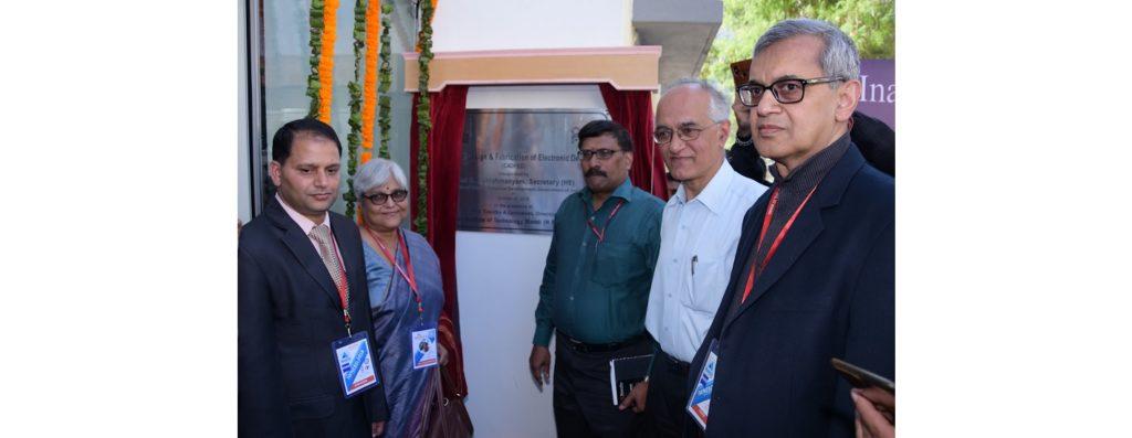
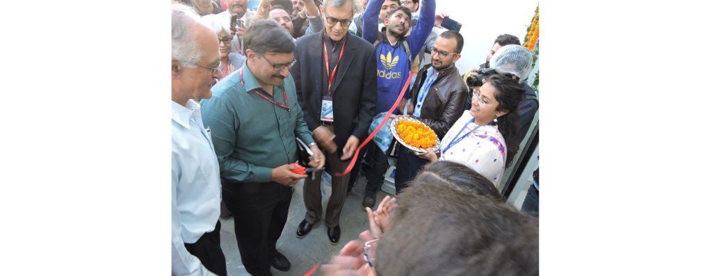
The high-end state-of-the-art C4DFED facility was inaugurated by Shri R. Subrahmanyam, Secretary (HE), Ministry of Human Resource Development (MHRD), Govt. of India on 31st October 2018.
The C4DFED center contributes to the advancement of the materials design plus testing for volatile, non-volatile memories, graphene, polymer nanocomposite and CNTs FETs design and fabrications, flexible electronics NEMS/MEMS sensors, photovoltaics, intelligent packaging, RF identification devices, bio-electronic interfaces, device prototyping along with interface between academia and semiconductor industries
News
Dr Vignesh Viswanathan, Applications Specialist (Materials Electron Microscopy) at Carl Zeiss, Singapore and his team will visit C4DFED and provide the application training on HIBL system from 1 April to 6 April 2019.
Dr Vignesh Viswanathan, Applications Specialist (Materials Electron Microscopy) at Carl Zeiss, Singapore and his team will visit C4DFED and provide the application training on HIBL system from 1 April to 6 April 2019.

APEER Image Processing Contest CARL ZEISS
Pagination
- Previous page
- Page 4
- Next page
About us
A vision of C4DFED Facility @ IIT Mandi A World-Class Dynamic Infrastructure and Toolset for Next Generation Integrated Circuits (IC’s) & Electronic Device Design & Fabrication Research and also technology development focusing on Semiconductor Industries. The School of Computing and Electrical Engineering.
Thematic Area C4DFED
Thematic Area C4DFED Facility IIT Mandi The C4DFED user facility is focused to produce the nano/micro electronics devices for specific users areas and applications and in that process will develop the core technology as well as techniques which will make...

