Instument image
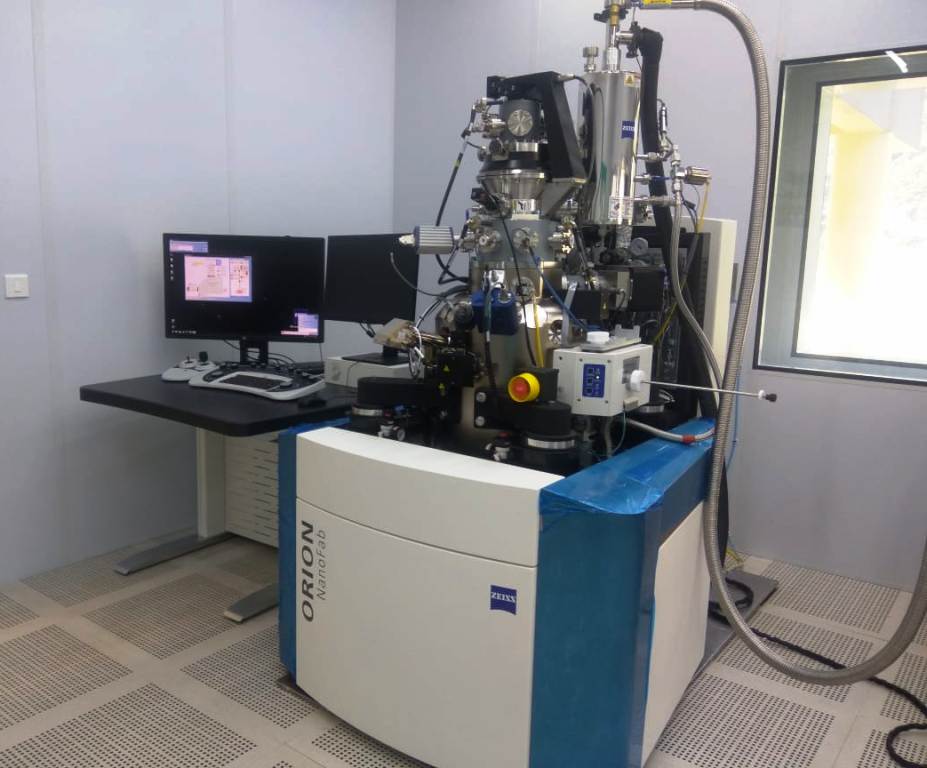
Company
Carl Zeiss Microscope
Model
ORION Nano Fab
Purpose
An emerging lithographic technique offers a promising alternative to electron beam lithography for fabricating new semiconductor devices with transistor fabrication below 10 nm both traditional and non-traditional resists. This allows pattering for them.